Atomic force microscopy (AFM) offers a potential solution for analyzing nanoplastics without the need for surface metallization. Unlike other microscopies, AFM operates on a different principle. It uses a rigid conductive tip attached to a cantilever (a long beam with a tip located at its apex) that interacts with the sample during measurement. The cantilever moves across the sample surface in three dimensions using a piezoelectric mechanism (the process of using crystals to convert mechanical energy into electrical energy or vice versa). The tip-sample interaction can be controlled to maintain a constant force or height, providing information on the sample’s interaction strength or height variations. An optical system detects the cantilever’s oscillations (repetitive or periodic variation, typically in time, of some measure about a central value (often a point of equilibrium) or between two or more different states), reconstructing the sample’s image based on the relative movement and tip-sample distance.
AFM can be used in contact mode, where the tip physically contacts the sample, or non-contact mode, where the tip remains a few nanometers away from the sample’s surface. Another mode, tapping mode, offers high resolution but requires a lever with a high elastic constant.
AFM utilizes various forces, such as van der Waals, electrostatic, magnetic, capillary, and friction forces, to generate images. It has been widely applied in characterizing nanoscale samples, providing additional characterizations beyond scanning electron microscopy (SEM).
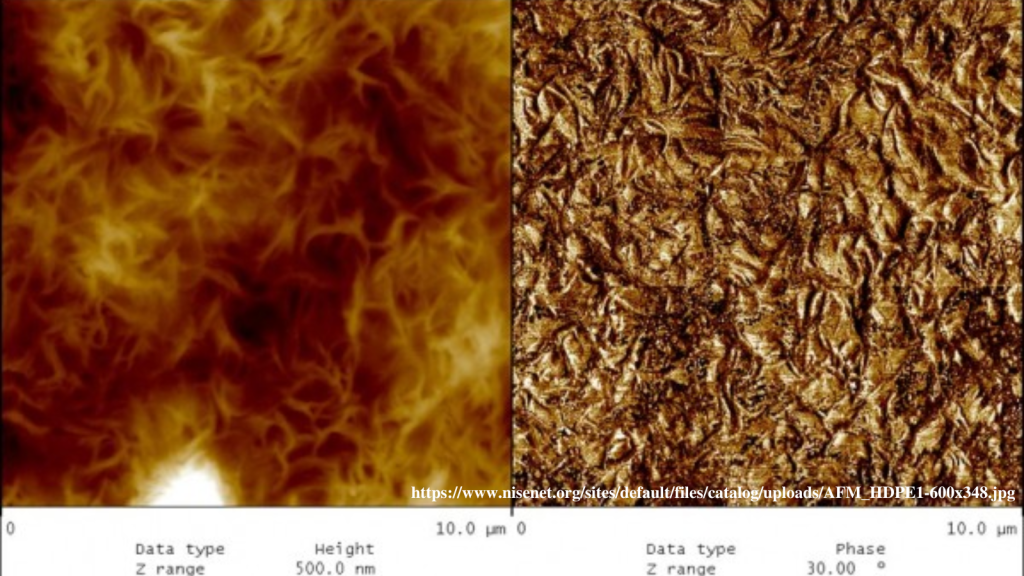
AFM offers several advantages, including high-resolution imaging, preservation of sample surface, suitability for non-conductive polymers like microplastics, and direct 3D imaging of polymer surfaces. AFM enables both quantitative measurements of surface roughness and qualitative analysis through nanoscale-resolution imaging of microplastics. One notable advantage of AFM is its exceptional scanning resolution in three dimensions, achieving resolutions as fine as ≤1 nm, depending on the size of the cantilever tip. This high-resolution capability allows for a thorough examination of the physical surface structure of microplastics, expanding the range of analysis previously unexplored. Furthermore, AFM surpasses scanning electron microscopy (SEM) in its ability to scan in three dimensions at the same level of resolution. Consequently, AFM is accomplished at detecting more detailed changes in surface roughness. However, AFM also has limitations, such as vulnerability to external contaminations and potential artifact formation during the interaction with the sample. To overcome these limitations, AFM can be combined with other analytical techniques (1, 2, 3).
Ref:
1. Won Joon Shim et al., 2017, “Identification methods in microplastic analysis: a review”, Anal. Methods, 2017, 9, 1384
2. Mariano S, Tacconi S, Fidaleo M, Rossi M and Dini L, 2021, “Micro and Nanoplastics Identification: Classic Methods and Innovative Detection Techniques”, Front. Toxicol. 3:636640. doi: 10.3389/ftox.2021.636640
By: Moe Thazin Shwe, SOLEN Research Associate – IPC Panel Member
Edited by: Hendra WINASTU, SOLEN Principal Associate – IPC Panel Coordinator
Date: 2 June 2023
Article#: SOLEN-IPC-0019

 Tiếng Việt
 日本語
日本語
Pingback: Transmission Electron Microscopy (TEM) and Microplastic (MP) - Solen
Pingback: Transmission Electron Microscopy (TEM) and Microplastic (MP) - SOLEN-IPC-016 - Solen